September 19, 2024
5 PCB Design Mistakes That Could Ruin Your Board
Share
BuildWithFlux


Let's dive in.
One of the most common mistakes in PCB design is not paying enough attention to trace width and spacing, especially in high-current or high-speed applications. If the trace is meant to carry high currents but it happens to be too narrow, it can result in thermal issues or even a failure of the circuit.
The width of your trace can be determined by things like; how much current it should carry without overheating or causing excessive voltage drops, Impedance control, and sensitivity of the signal running through it.
Flux makes routing high speed signals, such as USB data lines, easier by automatically performing coupled routing of the data lines (D+ and D-) and calculating the impedance of the pair based on the PCB stackup. This helps prevent reflections that can cause signal distortion, timing issues, and data corruption.
Flux Copilot can also help you calculate the appropriate trace width based on the current it needs to carry, while also considering the required impedance for high-speed signals. Just ask something like:
@copilot please recommend trace width for my VBUS.
Then copilot responses:
“For VBUS, typically a 5V supply in USB applications, let's assume a common scenario where you might anticipate a current of up to 1A. Using a temperature rise of 10°C, the general guideline for trace width on a 1 oz/ft² copper PCB is approximately 20-30 mils (0.5-0.8 mm) per amp of current.”
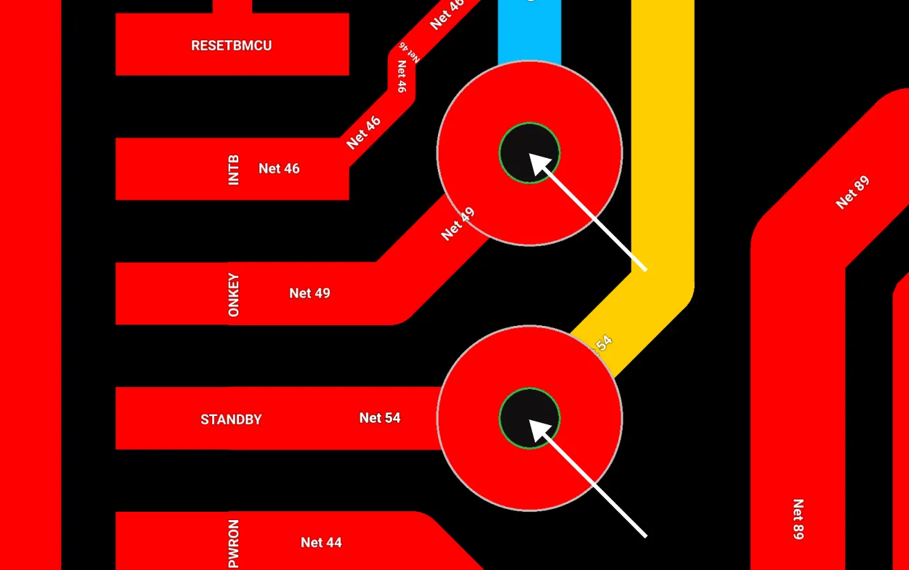
Vias are crucial for connecting different layers in a PCB, but choosing the wrong size or type can cause issues in both signal integrity and manufacturing. Blind, buried, and microvias are often used in high-density interconnect (HDI) boards, but these require careful consideration during design. For instance, microvias are perfect for compact designs, but if placed improperly, they can lead to poor layer transitions or increased inductance.
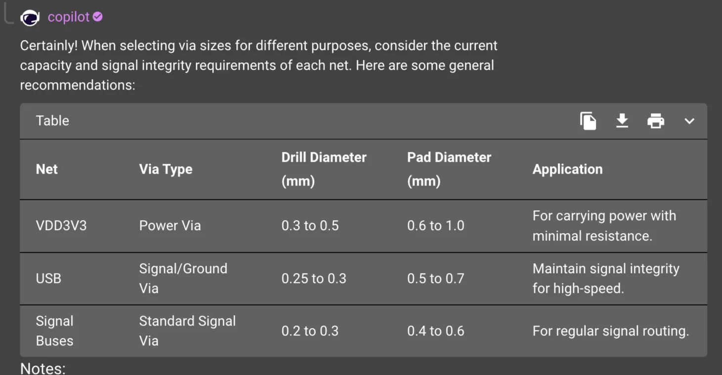
Flux let’s you set up your stackup where you add all the manufacturer capabilities. When you need some more advice on what stackup best suits your design, always feel free to ask copilot for some ideas, you could ask
@copilot in a table format recommend vias sizes that i can use for my VDD3V3, my USB, and the other signal buses?
Then here's the copilot response,
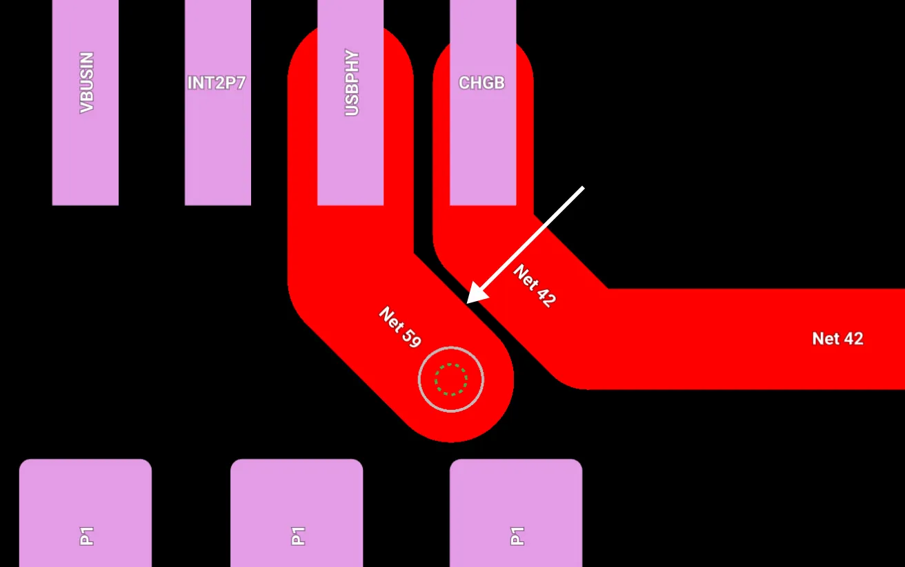
If you're routing a high-speed differential pair, such as USB or PCIe, through multiple layers, via stubs can cause signal reflections that degrade signal quality. A rule of thumb is to ensure via lengths are minimized, or even better, use back-drilling techniques to remove stubs, especially in high-frequency circuits.
Moreover, not all manufacturers support the same via sizes, so checking with your manufacturer early in the design process can avoid headaches later. Make sure to adhere to their capabilities, including the aspect ratio limits (via depth to diameter), to avoid costly redesigns e.g. 20:1 for PCBWay.
The layout of power and ground planes is another common area where mistakes are made. These planes act as the backbone of your circuit's stability, so a poorly designed plane can introduce noise, increase EMI, and degrade power delivery.
By default, Flux starts you off with a solid, contiguous ground plane since it is critical for minimizing noise and providing a low-impedance return path for high-speed signals. It is advisable to avoid creating islands which can cause severe signal integrity.
Example:
Imagine routing a high-speed signal across a split ground plane. The signal may cross the gap, creating a longer return path, which increases inductance and can lead to signal distortion or timing errors in critical circuits like clocks or data buses.
Similarly, power planes should be wide enough to handle the current required by each section of the circuit. For designs with sensitive analog circuits, it’s often a good idea to have separate power planes or split planes for analog and digital sections to avoid cross-talk and noise coupling.
Designing with manufacturability in mind is essential to ensure that your board can be built without issues. It’s easy to forget that the design rules you use in your ECAD tool may not fully align with your manufacturer’s capabilities, and this can result in delays or additional costs.
Flux provides users with pre-configured templates which align with most of the popular manufacture (e.g. PCBWay, JLCPCB, AISLER, LION Circuits, SEEED Studio and many more) capabilities so that users don’t have to worry about manually configuring things like trace widths, keepout, and other parameters. A good general rule of thumb is to always start new project using Flux manufacturer design rule templates
There are numerous DFM tips but here are some common ones to consider;
Using Flux manufacturer design rule templates will alert you when either of the manufacturer capabilities are violated even before sending your files for manufacturing saving you time.
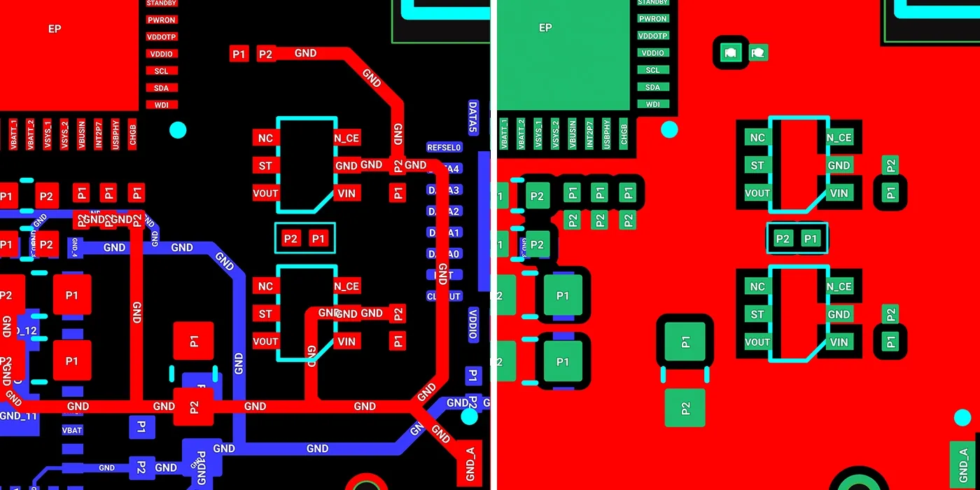
Decoupling capacitors are used to filter out noise and provide a stable voltage to ICs, especially in digital circuits where rapid switching causes power fluctuations. However, placing these capacitors too far from the pins of the IC can render them ineffective. It is advisable to place these decoupling capacitors as close as possible to the IC without violating the minimum spacing a manufacturer can work with.
Example:
In a typical microcontroller design, you should place decoupling capacitors (such as 0.1µF and 1µF) as close as possible to the VCC and GND pins. Ideally, the capacitors should be placed on the same layer as the IC to reduce parasitic inductance and ensure faster response times. Failure to do so can cause power integrity issues, leading to glitches or resets in your circuit.
Additionally, use vias sparingly when routing decoupling capacitors. Each via adds inductance to the path, which reduces the capacitor's ability to suppress high-frequency noise.
Before pressing that button to send your PCB design for manufacturing, it's worth taking a step back and performing a thorough review of your design. These design review steps can be quite a handful but what we have discussed above can be considered as the bare minimum. Flux manufacturer design rules makes it easy to ensure trace widths, appropriate via sizes, and manufacturer capabilities are considered when designing your board.
A thorough PCB design review can be a very daunting task, you might not be sure where to start or what checks to include in the review process. That is one of the reasons Flux’s AI lives in your project. You can use copilot to quickly check decoupling capacitors, power and grounding, ensuring compliance with industry standards, and even creating a stronger supply chain. To learn more about how you can use this tool, Sign up for Flux today.
Let's dive in.
One of the most common mistakes in PCB design is not paying enough attention to trace width and spacing, especially in high-current or high-speed applications. If the trace is meant to carry high currents but it happens to be too narrow, it can result in thermal issues or even a failure of the circuit.
The width of your trace can be determined by things like; how much current it should carry without overheating or causing excessive voltage drops, Impedance control, and sensitivity of the signal running through it.
Flux makes routing high speed signals, such as USB data lines, easier by automatically performing coupled routing of the data lines (D+ and D-) and calculating the impedance of the pair based on the PCB stackup. This helps prevent reflections that can cause signal distortion, timing issues, and data corruption.
Flux Copilot can also help you calculate the appropriate trace width based on the current it needs to carry, while also considering the required impedance for high-speed signals. Just ask something like:
@copilot please recommend trace width for my VBUS.
Then copilot responses:
“For VBUS, typically a 5V supply in USB applications, let's assume a common scenario where you might anticipate a current of up to 1A. Using a temperature rise of 10°C, the general guideline for trace width on a 1 oz/ft² copper PCB is approximately 20-30 mils (0.5-0.8 mm) per amp of current.”
Vias are crucial for connecting different layers in a PCB, but choosing the wrong size or type can cause issues in both signal integrity and manufacturing. Blind, buried, and microvias are often used in high-density interconnect (HDI) boards, but these require careful consideration during design. For instance, microvias are perfect for compact designs, but if placed improperly, they can lead to poor layer transitions or increased inductance.
Flux let’s you set up your stackup where you add all the manufacturer capabilities. When you need some more advice on what stackup best suits your design, always feel free to ask copilot for some ideas, you could ask
@copilot in a table format recommend vias sizes that i can use for my VDD3V3, my USB, and the other signal buses?
Then here's the copilot response,
If you're routing a high-speed differential pair, such as USB or PCIe, through multiple layers, via stubs can cause signal reflections that degrade signal quality. A rule of thumb is to ensure via lengths are minimized, or even better, use back-drilling techniques to remove stubs, especially in high-frequency circuits.
Moreover, not all manufacturers support the same via sizes, so checking with your manufacturer early in the design process can avoid headaches later. Make sure to adhere to their capabilities, including the aspect ratio limits (via depth to diameter), to avoid costly redesigns e.g. 20:1 for PCBWay.
The layout of power and ground planes is another common area where mistakes are made. These planes act as the backbone of your circuit's stability, so a poorly designed plane can introduce noise, increase EMI, and degrade power delivery.
By default, Flux starts you off with a solid, contiguous ground plane since it is critical for minimizing noise and providing a low-impedance return path for high-speed signals. It is advisable to avoid creating islands which can cause severe signal integrity.
Example:
Imagine routing a high-speed signal across a split ground plane. The signal may cross the gap, creating a longer return path, which increases inductance and can lead to signal distortion or timing errors in critical circuits like clocks or data buses.
Similarly, power planes should be wide enough to handle the current required by each section of the circuit. For designs with sensitive analog circuits, it’s often a good idea to have separate power planes or split planes for analog and digital sections to avoid cross-talk and noise coupling.
Designing with manufacturability in mind is essential to ensure that your board can be built without issues. It’s easy to forget that the design rules you use in your ECAD tool may not fully align with your manufacturer’s capabilities, and this can result in delays or additional costs.
Flux provides users with pre-configured templates which align with most of the popular manufacture (e.g. PCBWay, JLCPCB, AISLER, LION Circuits, SEEED Studio and many more) capabilities so that users don’t have to worry about manually configuring things like trace widths, keepout, and other parameters. A good general rule of thumb is to always start new project using Flux manufacturer design rule templates
There are numerous DFM tips but here are some common ones to consider;
Using Flux manufacturer design rule templates will alert you when either of the manufacturer capabilities are violated even before sending your files for manufacturing saving you time.
Decoupling capacitors are used to filter out noise and provide a stable voltage to ICs, especially in digital circuits where rapid switching causes power fluctuations. However, placing these capacitors too far from the pins of the IC can render them ineffective. It is advisable to place these decoupling capacitors as close as possible to the IC without violating the minimum spacing a manufacturer can work with.
Example:
In a typical microcontroller design, you should place decoupling capacitors (such as 0.1µF and 1µF) as close as possible to the VCC and GND pins. Ideally, the capacitors should be placed on the same layer as the IC to reduce parasitic inductance and ensure faster response times. Failure to do so can cause power integrity issues, leading to glitches or resets in your circuit.
Additionally, use vias sparingly when routing decoupling capacitors. Each via adds inductance to the path, which reduces the capacitor's ability to suppress high-frequency noise.
Before pressing that button to send your PCB design for manufacturing, it's worth taking a step back and performing a thorough review of your design. These design review steps can be quite a handful but what we have discussed above can be considered as the bare minimum. Flux manufacturer design rules makes it easy to ensure trace widths, appropriate via sizes, and manufacturer capabilities are considered when designing your board.
A thorough PCB design review can be a very daunting task, you might not be sure where to start or what checks to include in the review process. That is one of the reasons Flux’s AI lives in your project. You can use copilot to quickly check decoupling capacitors, power and grounding, ensuring compliance with industry standards, and even creating a stronger supply chain. To learn more about how you can use this tool, Sign up for Flux today.


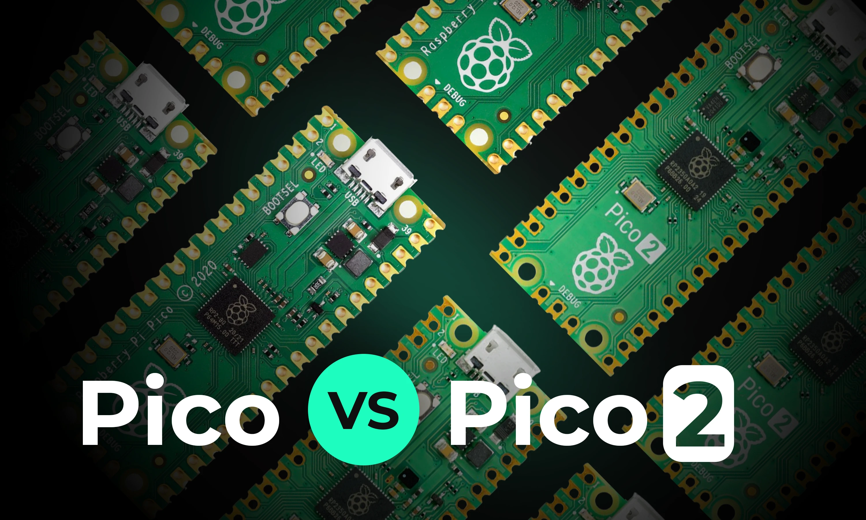
This article will explore the key differences between the original Raspberry Pi Pico and the new Raspberry Pi Pico 2, focusing on the most significant enhancements and what remains unchanged.

From programming to hardware connections, this ATtiny85 comprehensive guide provides everything you need to know to get started. Read on and start exploring the endless possibilities of this tiny yet mighty microcontroller.

For months, we’ve been adding new features and functions to Copilot to help make it the most powerful AI for hardware design in the world. Today, we’re announcing what might be the biggest upgrade yet: Copilot Vision.

Designing a PCB is an intricate and engaging process that plays a pivotal role in electronics. The steps and tips provided in this article are not exhaustive but will certainly help you in your journey to designing effective and efficient PCBs. Armed with these insights, it's time to bring your electronic ideas to life with your own PCB designs
Practical guide to writing prompts that get quality results from Flux. We’ll talk about the anatomy of a good prompt and how you can use different LLMs to come up with a great prompt.

Focusing on Arduino Mega, Micro, and Uno, the blog details how the Mega 2560 stands out with its extensive memory and numerous I/O pins for sophisticated projects.

If you're looking to improve your understanding of schematic diagrams, this article is the perfect starting point. Let's explore the crucial role of circuits and components schematics in translating conceptual electrical designs into physical printed circuit board assemblies (PCBAs).

Want to design your own macropad? Discover how to create one using the Raspberry Pi Pico 2 and Flux's AI Auto-Layout. From schematics and components to PCB layout and firmware, we’ve got you covered. Boost your productivity with a custom macropad—start building today!

This blog compares AI capabilities across Flux.ai, Altium, KiCad, and EasyEDA to answer engineers’ highest-intent questions about modern PCB design. It explains why Flux.ai currently delivers the strongest end-to-end AI workflow in the ECAD space.

Electronics, whether in a phone or an industrial motor, face potential threats from unchecked electrical currents. Our guide introduces protection circuits, the essential safeguards that monitor and respond to such electrical anomalies.

Discover how CAD Librarians can leverage Flux’s key capabilities—AI Part Imports, Component Updates, Live Pricing, and JEP30 Export—each tailored to meet the specific demands of maintaining PCB libraries.

Today, we’re excited to introduce AI Auto-Layout, powered by Flux Copilot. This is the next step toward full layout automation. With just one click, Copilot tackles the repetitive task of routing your board, delivering clean, human-like results that are easy to work with and iterate on.