February 7, 2025
Prototyping vs. Production-Ready Electrical Engineering
Share
BuildWithFlux


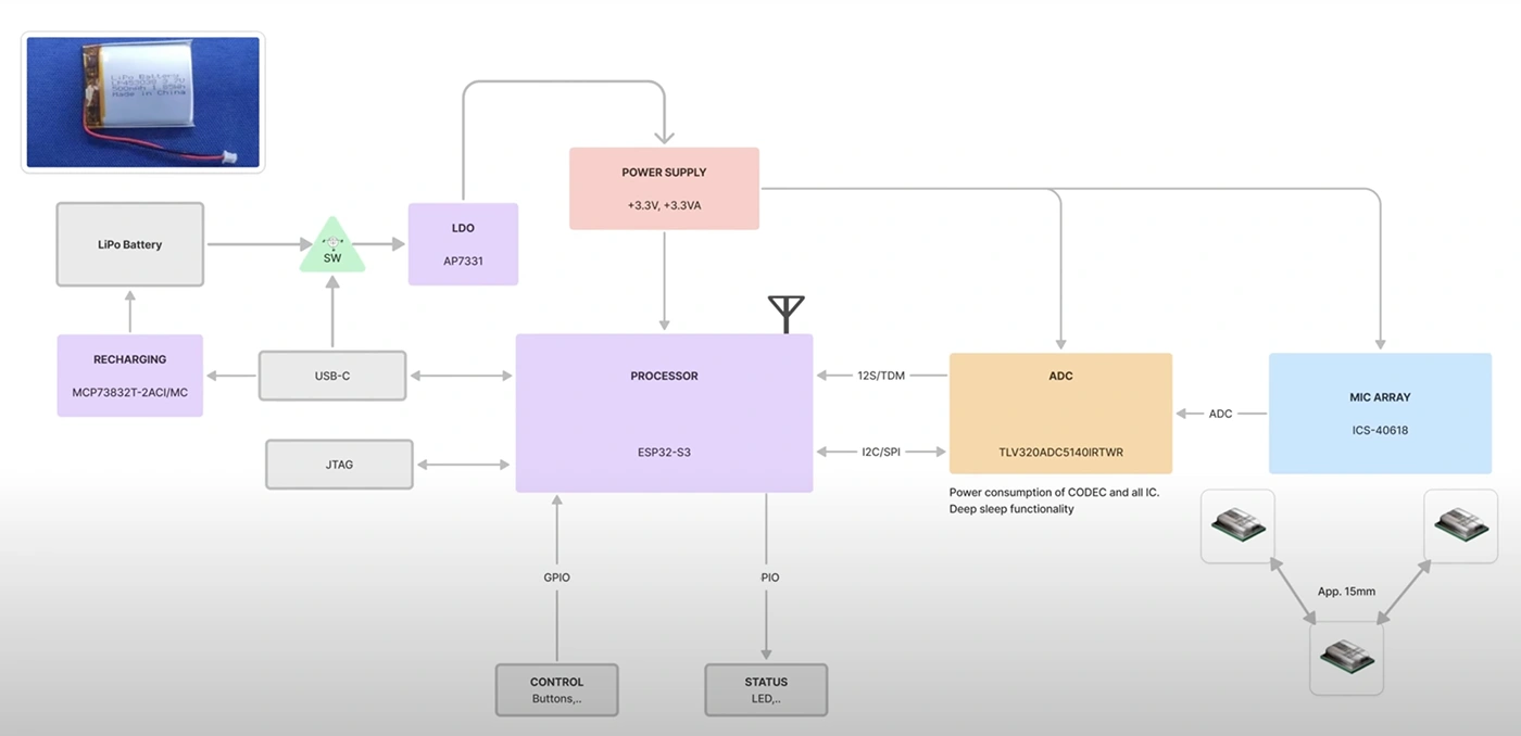
Let's break it down with a case study: a wearable AI pendant built around the ESP32-S3. It packs a microphone array, a LiPo battery with USB-C power, and a PCB antenna into a compact, power-efficient design. How would a design intended for a few prototypes differ from one built for mass production? More importantly, how can a designer transition from one to the other?
A design for prototyping is likely to start with an ESP32 development board, stacking breakout modules for power, audio, and sensors, and wiring everything together on a protoboard. This modular approach speeds up development, allowing rapid iteration and debugging. However, the result is often bulkier and less optimized for power efficiency and performance.
A production-ready design follows a different path. It begins with a block diagram, mapping out power distribution, signal paths, and communication protocols. Instead of separate breakout boards, all functions are integrated into a single custom PCB. This minimizes component count, optimizes trace routing, and ensures better signal integrity, ultimately leading to a leaner, more reliable system.
How to Transition: To move from a prototype to a production-ready design, start by identifying frequently used breakout board components and replace them with equivalent ICs that can be integrated directly onto the PCB. Use search tools like Digikey’s filter or Copilot to narrow the search and check the reference design or application note in each datasheet you are evaluating. Use the prototype to refine the design before committing to a custom layout.
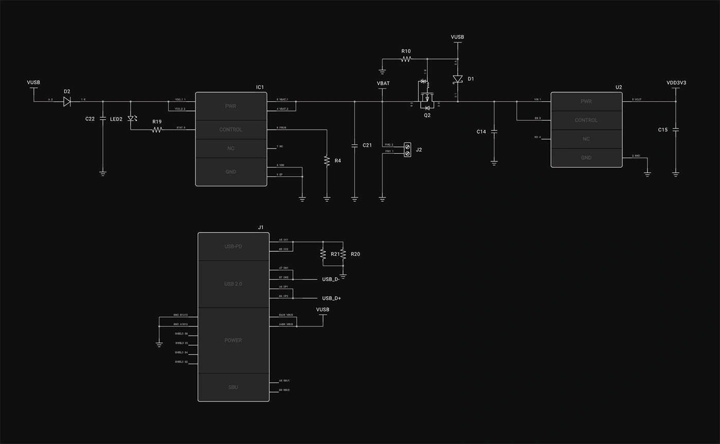
A prototype design might use an AMS1117 linear regulator because it’s easy to wire up and doesn’t require extra components. A generic charging module is typically added, setting up a functional but inefficient system that dissipates excess energy as heat.
A production-ready design optimizes every power stage. The MCP73832T charging IC is chosen with a charge current precisely set based on the battery’s capacity. A MOSFET-based power switch ensures seamless transitions between USB and battery power, while a carefully selected low-dropout regulator (LDO) or buck converter maximizes efficiency, extending battery life and reducing thermal issues.
How to Transition: Instead of relying on modular solutions, select integrated power management ICs suited for your voltage and current requirements. Optimize power paths by minimizing unnecessary regulators and designing efficient layouts to reduce power loss.
A prototype design may rely on the ESP32’s built-in PCB antenna, which works for initial development but can suffer from signal degradation due to poor placement and interference.
A production-ready design requires careful RF planning. The ground plane is optimized, and impedance-controlled traces ensure signal integrity. A matching network is tuned to improve impedance matching, reducing signal reflection and maximizing transmission efficiency.
How to Transition: Follow manufacturer guidelines for PCB antenna placement and matching networks. There are many resources and simulation software's to ensure accurate design like Ansys. Use impedance-controlled stack-ups in your PCB layout to ensure signal stability and range.
A prototype might connect MEMS microphones directly to the ESP32-S3’s ADC, which works but is susceptible to noise. Single-ended connections can pick up unwanted interference, degrading signal quality.
A production-ready design accounts for signal integrity. Differential microphone routing reduces noise, and DC-blocking capacitors are selected to fine-tune frequency response. Impedance-matched traces ensure reliable signal transmission, while an external ADC is used for higher fidelity audio.
How to Transition: If audio quality is a key requirement, incorporate differential microphone routing and external ADCs early in the design. Use simulation tools to validate signal integrity before committing to the layout. Always check the frequency response characteristics of the ADC and Microphone.
PCB design benefits from automation, but knowing when and how to use AI Auto-Layout is key. A prototype design might rely on auto-routing for the entire board, allowing for quick prototyping and iteration. This speeds up development but may introduce unnecessary vias, tangled traces, and potential EMI issues.
A production-ready design takes a hybrid approach. High-speed, sensitive signals, and power traces are manually routed to ensure signal integrity. Once these critical traces are placed, AI Auto-Layout handles the remaining connections, reducing design time while maintaining quality.
How to Transition: Start by routing critical signals manually, especially high-speed traces and power connections. Use AI Auto-Layout for non-critical traces, ensuring design efficiency without compromising quality.
Prototyping and production-ready designs share the same fundamental principles: understanding tradeoffs, optimizing efficiency, and refining designs. A prototype prioritizes flexibility and quick iteration, while a production design optimizes for manufacturability, longevity, and performance.
Neither approach is inherently better; they serve different purposes. The best designers learn from both worlds. Those developing prototypes can incorporate creative design methodologies, while those working toward production can embrace the structured and precision of integrated design.
At the end of the day, electrical engineering isn’t about rigidly following a set of rules—it’s about making smart, defensible decisions based on the constraints at hand. Whether you're building a quick prototype or refining a production-ready device, the key is knowing the why behind every choice.
Want to see a full breakdown of this project? Check out the complete design walkthrough!


Avoid costly errors in your PCB design with these expert tips! Discover the 5 most common mistakes in trace width, vias, power planes, and more. Learn how Flux’s AI Copilot helps you catch these issues early, ensuring your board is ready for manufacturing.
This blog highlights CES 2025 showcased projects, offering insights on how to recreate them using Flux. With Flux AI-driven design tools, component library, and customizable templates, engineers and hobbyists can build inspired hardware like wearables, drones, EV components, portable chargers, and solar devices.

A case study: Learn how Agri-iO reimagined farm automation with custom hardware designed in Flux.

Streamline component research with Flux Copilot. Copilot links to components for quick part research, offering multiple options tailored to your needs, and find part alternatives effortlessly without switching between tabs and platforms.
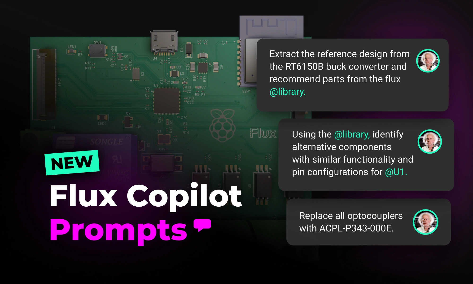
With the latest release of Copilot it isn’t just smarter—it’s hands-on, placing components and applying bulk changes to your project instantly. But to get the most out of it, knowing how to craft the right prompt is key.

We’ve been so amazed with the ways you’ve used Copilot to brainstorm, debug, and conduct part research that we’ve compiled some of our favorite prompts you can copy and paste, or modify for your own use!


With Flux, enterprises can take their architectural ideas and use AI to transform those ideas into actionable items. With Copilot, your enterprise can generate schematics, perform AI design reviews, and even identify PCB technology, budgets, and timelines well in advance of any manufacturing.

Discover how CAD Librarians can leverage Flux’s key capabilities—AI Part Imports, Component Updates, Live Pricing, and JEP30 Export—each tailored to meet the specific demands of maintaining PCB libraries.